Customer background
Company Location: Iran
Application: Consumer Electronics
Field: Drone
Service: FR4 PCB Manufacturing
Project challenge
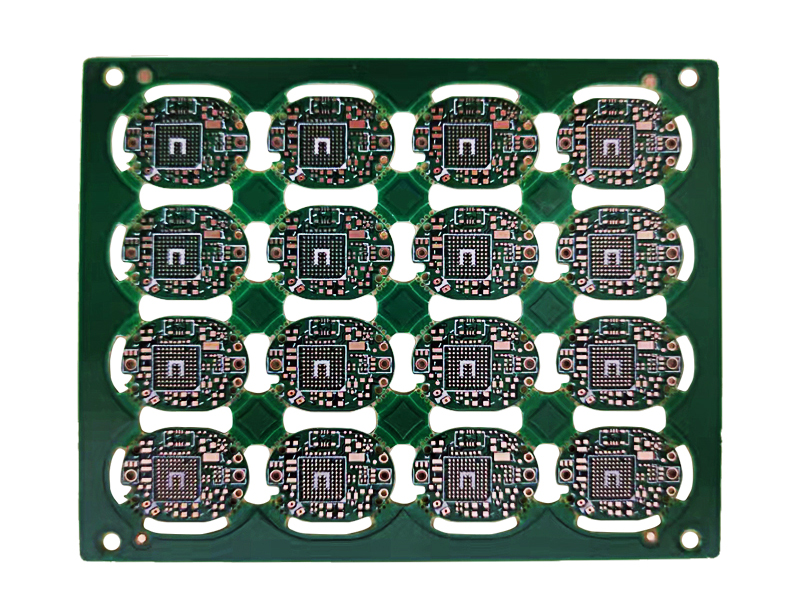
The veneer size of this board is very small, 6 layers but the thickness of the board is only 0.8mm. According to the customer's information, the process of using holes in the board is required. We use resin to plug the hole and then plate the cap, which can not only make the via hole on any pad and BGA, but also will not affect the subsequent SMT. Fill the via hole with resin first, dry the resin and grind it flat, and then plate copper on the surface of the resin, so that there is no trace of via hole on the appearance, and it will not affect the soldering. The performance and effect of the hole-in-disk process are far better than "via hole solder mask" and "via hole plugging oil". There is neither the problem of yellowing of the hole of via hole solder mask, nor the problem of poor SMT soldering performance caused by easy oil leakage of via hole plug oil.
6 layers immersion gold plate hole PCB manufacturing Process
1. Customer places an order
Customers place orders according to their actual needs and put forward specific requirements. The processing plant will evaluate through its own capabilities, and the two parties will negotiate to determine various production details.
2. Customers provide production materials
After the customer decides to place an order, he will provide the PCB processing factory with a series of documents, such as the PCB electronic documents required for production. Then our engineers conduct DFM inspection and make Working Gerber, the customer confirms that there is no problem, and start the production of material selection.
3. Select raw materials
The PCB processing factory selects relevant raw materials from the designated supplier according to the documents and materials provided by the customer.
4. Incoming material inspection
Before PCB processing, all raw materials to be used shall be subject to strict quality inspection to ensure that they are qualified before being put into production.
5. PCB production
During PCB processing, in order to ensure the quality of production, our factory will conduct quality sampling inspections throughout the entire manufacturing process.
6. PCB test
The PCB processing factory conducts strict product testing, and the PCB boards that pass the test are delivered to customers.
7. Packaging and after-sales service
After the PCB processing is completed, the product is packaged and delivered to the customer to complete the entire PCB processing work.
Results and Benefits
After receiving the customer's Gerber file, we quickly responded to the customer's order and completed the order within 1.5 weeks.
Before shipment, we will conduct AOI and function test. Guarantee that the quality of the shipped products is all qualified.
We won’t charge the tooling fee again next production for the same projects. The unit price also can cheaper. And we can manufacture faster for mass production.
Linda
I am Linda, sales team leader of Best Technology, 5 years’ experience in PCB. If you want to custom PCB and PCBA, please feel free to contact me to ask any questions.