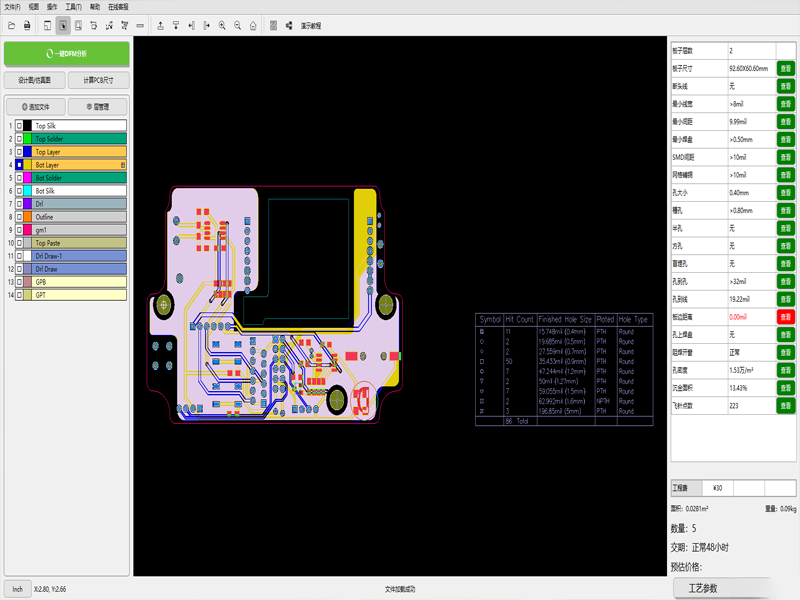
Our engineers
provide free PCB file inspections to ensure there are no missing components or
incorrect structures, and to check whether these file designs are within the
capabilities of our production process.
Before mass
production, we recommend PCB prototype manufacturing. Through this step, check
whether the design of the printed circuit board is reasonable, whether the
function can be used normally, and whether the quality meets the requirements
of mass production.
Can reduce production cost for customers.
Can help customers optimize the design of
the circuit board.
It can bring technological breakthroughs to
customers' innovations.
Once the prototype is validated, we will
enter the formal production phase.
We will have all the components of the Bom
ready at the same time as the PCB is produced so that assembly can begin
immediately after the PCB is manufactured.
All circuit boards will be 100% inspected
and tested. We will provide a shipment report for your review.
IPC-A-600F Class II. Acceptance Criteria
IPC-TM-650 Class II. Test Method Standard
ISO9001,ISO13485,ISO16949,AS9100C,ROHS,UL
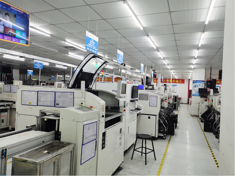
Step 5: PCB Assembly
We can provide you with a complete turnkey
PCB assembly, working with you from the design stage to product completion,
saving you time and trouble.
All components are original, no counterfeit
or gray market used components are used.
The lead time for PCB assembly prototypes
can be as fast as 24 hours. Mass production can also provide fast assembly
process within 3-4 days.
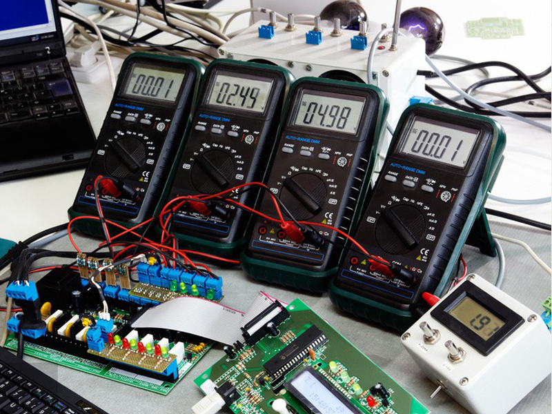
Step 6: Inspection and Testing
PCBA inspection and testing is an important
means to control product quality in the entire production process of PCBA
processing. With the improvement of the pass rate of products, the pass rate of
products will be greatly improved.
In our production and processing process,
we have many inspection methods to ensure the production quality of SMT patch
processing, DIP plug-in post-welding and other processing.
SPI detector
Manual visual inspection
Digital microscope
SMT First Article Inspection
AOI automatic optical inspection
X-ray
ICT test
FCT function test
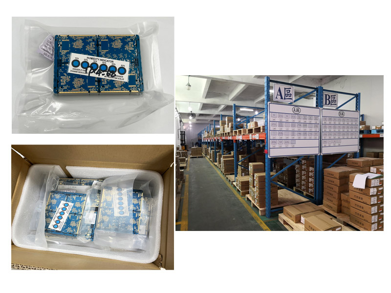
Step 7: Package and Shipment
Package: We use vacuum packaging and outer
packaging, cardboard boxes and thick cartons for all PCB products. This ensures
that the packaged PCB products are not easily damaged during delivery.
Shipment: We cooperate with world famous
freight forwarders: DHL, FedEx, UPS, TNT. This ensures the shortest lead times
and the safe and fast arrival of the PCB at the customer's side.
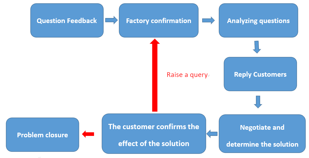
Step 8: After-sale service
Every PCB made in our factory enjoys dedicated
after-sales service. If you receive the goods and cause board problems due to
our fault, you can give us after-sales feedback. The after-sales engineer will
confirm the relevant problems and contact you in time to communicate and deal
with them.
Talk to a PCB Manufacturer Expert today
We look forward to working with you side by side, to be a long-term partner whom you can trust.