It takes a little time to make EQ and confirm the working Gerber, and using the thick film process and the silver palladium line conductor. The entire production time is relatively urgent.
How to serve?
Pulse laser or continuous laser can be used in laser processing for cutting holes, and pulse laser is generally used for scribing to reduce the thermal impact of laser partial heating on ceramic substrates.
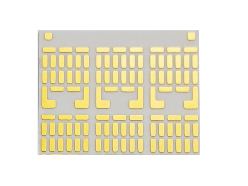
The silver paste forms a circuit on the surface of the alumina ceramic substrate through the screen printing process, and the organic components in the silver paste are discharged through sintering. At the same time, the glass and silver powder are softened, and the silver is bonded to the alumina ceramic substrate to form a circuit.
The substrate is sintered at a high temperature of 850~900°C during processing.
Results and Benefits
The manufacture of ceramic circuit boards was completed within the stipulated time, and the products were shipped to customers smoothly.
The customer is very satisfied with our service, and our company also produces for him in mass production.
Jennifer
I am Jennifer, sales team leader of Best Technology, 5 years’ experience in PCB. If you want to custom Ceramic PCB and PCBA, please feel free to contact me to ask any questions.