Customer background
Company Location: USA
Application: Automotive Electric Power
Field: New energy vehicles
Service: PCB Manufacturing
Project background
Our client is an electric vehicle company, and their automotive equipment needs Thick Copper PCB.
BETON circuit, with its unique technical strength and advanced equipment, has cooperated with the customer's supporting supplier for more than 3 years, and is deeply favored by customers, and it is not stingy to offer high scores......
At that time, the customer was not short of suppliers, and many circuit board factories were cooperating, but there were always problems of one kind or another, some samples were NG, and some samples passed, but when mass production, some parts always reached Customers are very distressed if they do not meet the requirements......
In the industry, BETON circuit has a good reputation and brand effect, so customers found us. Through more than 10 years of experience in the production of special tolerance boards, coupled with the professional communication and communication of the technical team, BETON circuit has set up a project discussion and prevention plan , Proofing to small-batch trial production verification, one-time pass, every time customers talk about this case, they praise BETON circuit!
BETON circuit is mainly engaged in double-sided and multi-layer high-precision circuit boards. What we pursue is stable and reliable quality, which can create certain value for customers, and serve customers with focus, professionalism and efficiency, and provide diversified product types and processes. Advanced technology, relatively fast delivery speed and fast and convenient service are our mission!
Project challenge
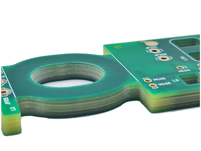
Due to the thicker copper thickness, thick copper boards bring a series of processing difficulties to PCB processing, such as the need for multiple etching, insufficient glue filling on the pressure plate, cracking of the inner pad of the drilled hole, and difficulty in ensuring the quality of the hole wall, etc.
Thick Copper PCB manufacturing Process
1. Selection of circuit board materials
High Tg sheet is recommended (S1000-2)
For thick copper circuit boards, due to the thicker copper thickness, its thermal conductivity is stronger. When mounted under the same conditions, ordinary Tg boards have problems such as layer explosion and white spots compared with high Tg boards.
2. Drilling
For thick copper circuit boards, due to the thicker copper and the superimposition of each layer, the copper is already at a large thickness. When drilling, the drill will be worn or broken for a long time in the board, which will further affect The quality of the hole wall will further affect the reliability of the product.
3. Circuit
For thick copper circuit boards, due to the thicker copper thickness, the processing difficulty is greater than that of ordinary boards when etching circuits. Therefore, increasing the line width and spacing in the design will help reduce the degree, and it will also greatly improve the lamination filling.
4. Lamination
For thick copper circuit boards, because the copper thickness is thicker, the thicker the copper thickness, the deeper the line gap. In the case of the same residual copper rate, the required amount of resin filling will increase accordingly with prepreg (PP) to meet the glue filling. When the resin is less, it will easily lead to lack of glue layering and poor thickness uniformity;
Due to the superposition effect of the inner layer circuit and the limitation of resin flow during lamination of the thick copper circuit board, the area with a high residual copper rate after lamination will be compared with the area with a low residual copper rate.
The thickness of the circuit board is uneven. Therefore, the uniformity of copper laying on the inner layer should be improved as much as possible during design.
5. Solder mask
For thick copper circuit boards, due to the thicker copper thickness, problems such as substandard ink thickness, vertical flow, false copper exposure and air bubbles are prone to occur during solder mask production. It is realized by welding printing and double exposure in the industry. Our company now has electrostatic spraying equipment to support the effect better.
Results and Benefits
Before shipment, we also did a Hi-Pot Test, using a metallographic copper thickness tester and a microscope to test the thickness of trace copper and hole copper to ensure that the hole copper thickness meets customer requirements.
Our professional engineering team and customers discuss manufacturing difficulties in a timely manner, and jointly solve problems that arise, which shortens the entire production time by half. Let customers put it into use as soon as possible, increasing their automotive equipment production capacity.
Linda
I am Linda, sales team leader of Best Technology, 5 years’ experience in PCB. If you want to custom PCB and PCBA, please feel free to contact me to ask any questions.